1. UART CPU implementation
Related reference articles:
RISC-V teaching plan
The RISC-V UART1 module is the same as the physical layer of the general UART, except that it adds the RIB read and write registers of the connection bus to configure some parameters (such as parity bits).
Because the speed of the two ends of the UART is different, for example, the FPGA system clock frequency is 50 MHz, and the common baud rate of the UART is 115200 Hz, so FIFOs are added on both the transmit and receive ends. The specific UART1 module design is shown in Figure 1. Here rx and tx represent receive, receive and transmit, respectively. phy refers to the physical layer, in this module, only the sending and receiving functions are completed. The buffer module connects the physical layer to the FIFO. The transceiver module passes the parameters configured by the register to the receiving and sending modules respectively. The RIB_UART1 module is connected to the bus to complete the reading and writing of UART1 related registers.
As you can see, the hierarchical structure of the modules makes the connection between the modules clear. If you need to expand another UART later, it is very convenient to add on the basis of the current UART module, only a small part of the modification is required, such as the address chip selection on the bus, and other parts can be used directly.

Figure 1 UART1 module design
Add the address and chip selection of UART1 to the bus as shown in Figure 2, and the base address parameters of UART1 as shown in Figure 3.

Figure 2 Adding a chip select in the bus

Figure 3 Add UART1 base address
The UART1 interrupt is also handled uniformly by the external platform-level interrupt handler (PLIC), so UART1 is also assigned a unique PLIC ID, as shown in Figure 4.
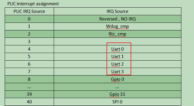
Figure 4 Partial PLIC ID assignment
Figure 5 shows the UART1 interrupt request in the PLIC.
Figure 5 Interrupt request of UART1 in PLIC
2. UART1 interrupt software engineering
On the basis of the PLIC software construction and the GPIO and PWM software engineering in the external interrupt source, only the newly added parts will be explained here. The previous PLIC software engineering details are shown in Sections 18-21 in the RISC-V teaching plan (click here ), as shown in Figure 6.
Figure 6 PLIC-related articles in the RISC-V teaching plan
Next, we will introduce the header files used by the UART1 project: platform.h and fii_uart1.h.
- Platform.h
Because when setting interrupts, not only the interrupt-related registers of UART1 need to be set, but also need to open interrupts and set priorities at the PLIC layer, so the offset of UART1 needs to be added in platform.h, where the offset of UART1 is based on The definition of different external interrupt sources on the address map is shown in Figure 4.
//=============================UART definition============================
#define INT_UART0_BASE 4
#define INT_UART1_BASE 5
#define INT_UART2_BASE 6
#define INT_UART3_BASE 7
//============================UART definition END==========================
- Fii_uart1.h
Fii_uart1.h defines the offset of the base address of UART1, as well as related parameters and the UART1 interrupt initialization function. For the specific explanation, see the following code.
#include "fii_types.h"

//UART1 base address offset
#define UART1_OFFSET 0X1000

//Offset of UART1 relative to UART base address
#define UART1_REG(offset) (*(volatile unsigned int *)(UART_BASE + UART1_OFFSET + offset))

#define UART1_TX_DATA 0X00              //Transmit data register offset
#define UART1_RX_DATA 0X04              //Receive data register offset

#define UART1_TX_CTRL 0X08              //Transmit control register offset
#define UART1_RX_CTRL 0X0C              //Receive control register offset

#define UART1_IE 0X10                   //Interrupt enable register offset
#define UART1_IP 0X14                   //Interrupt suspension register offset
#define UART1_IC 0X18                   //Interrupt clear register offset
#define UART1_DIV 0X1C                  //Baud rate divider register offset
#define UART1_LCR 0X20                  //Parity check register offset
#define UART1_VER 0X24                  //version register offset

#define UART1_TX_FIFO_FULL 0X80000000   //The FIFO empty mask in the transmit data register
#define UART1_RX_FIFO_EMPTY 0X80000000  //The mask of FIFO full in the receive data register
#define UART1_DATA_MASK 0XFF            //The mask of the 8-bit data in the transmit and receive data registers

#define UART1_TXEN 0X1                  //Transmit enable mask in transmit control register
#define UART1_RXEN 0X1                  //The mask of receive enable in the receive control register

//relative displacement of UART1 interrupt enable
#define UART1_TXWM_MASK 0X0
#define UART1_RXWM_MASK 0X1
#define UART1_PERROR_MASK 0X2

// used to set the mask for parity in the LCR register

#define NO_PARITY 0X0
#define ODD_PARITY 0X28
#define EVEN_PARITY 0X18
#define MARK_PARITY 0X8
#define SPACE_PARITY 0X38

// div register baud rate calculation formula:
// (50,000,000 / target baud rate) - 1
// eg 115200 Hz baud rate, 50 MHz clock frequency, 50_000_000/115200 = 434, div = 434 - 1 = 433 = 0x1b1
// Here are some commonly used baud rates that can be directly written to the div register

#define BAUD_RATE_115200 0X1B1
#define BAUD_RATE_57600  0X363
#define BAUD_RATE_38400  0X515
#define BAUD_RATE_19200  0XA2B
#define BAUD_RATE_14400  0XD8F
#define BAUD_RATE_9600   0X1457
#define BAUD_RATE_1200   0XA2C2

//=================================================================================

//Enumeration defines interrupt enable
typedef enum {
    UART1_IRQ_DIS = 0,
    UART1_IRQ_EN
} E_UART1_IRQ_SW;

//enumeration defines the data stop bit
typedef enum {
    UART1_NSTOP_1 = 0,
    UART1_NSTOP_2
} E_UART1_NSTOP;

//Separate the bits of the TXCTRL and RXCTRL registers to facilitate direct access to the transmit/receive interrupt watermark threshold
typedef union
{
    struct
    {
        unsigned int reserved1 :16;
        unsigned int rxwm_bit :3;
        unsigned int reserved2 :13;
    }bit;

    unsigned int rxctrl_reg;

}E_RXCTRL;

typedef union
{
    struct
    {
        unsigned int reserved1 :16;
        unsigned int txwm_bit :3;
        unsigned int reserved2 :13;
    }bit;

    unsigned int txctrl_reg;
}E_TXCTRL;

//=================================================================================

//Declare the UART1_IRQ_register function for UART1 interrupt initialization
void UART1_IRQ_register( u32_t uart1_baud_rate, u32_t uart1_parity, u32_t irq_mask,
                        E_UART1_NSTOP nstop, E_RXCTRL rxwm,
                        E_TXCTRL txwm, E_UART1_IRQ_SW uart1_sw);

//===============================
Here need to add knowledge about union and struct. Because the watermark threshold in txctrl and rxctrl occupies 3 bits, struct is required to access variables per bit in C language, as shown in the following code example.
struct {
    unsigned int reserved1 :16;
    unsigned int txwm_bit :3;
    unsigned int reserved2 :13;
}bit;
It can be seen that the variable bit is divided into three parts, arranged in order, bits 0-15 are reserved, bits 19-31 are also reserved, and bits 16-18, the interrupt watermark threshold can be accessed separately. The reason why a union is added outside the struct is because the union can store different data types at the same memory address. After adding the union, you can access either the individual 3-bit data or the entire variable together. The code is as follows:
typedef union {
    struct {
        unsigned int reserved1 :16;
        unsigned int txwm_bit :3;
        unsigned int reserved2 :13;
    }bit;

    unsigned int txctrl_reg;
}E_TXCTRL;
You can see that txctrl_reg is a 32-bit variable, and txwm_bit is a data with only 3 bits. When accessing, you can pass the following code:
E_TXCTRL txwm;
txwm.bit.txwm_bit = 0x3;
UART1_REG(UART1_TX_CTRL) = txwm.txctrl_reg;
The example here is to set bits 16-18 of txwm to 3, and then the other reserved areas remain unchanged, and the entirety is assigned to the txctrl register. Here E_TXCTRL is an alias for unsigned int defined with typedef.
Engineering code download: