1. GPIO interrupt source
Related reference articles:
RISC-V teaching plan
In PLIC (PLIC introduction click here ), among the external platform-level interrupt sources, there are a total of 32 GPIO interrupt sources, and the interrupt IDs are 8-39. The first 8 bits of each group of GPIO (there are currently 4 groups of GPIO, namely GPIO A, GPIO B, GPIO C, and GPIO D) can be set as the interrupt source. For example, interrupt ID 16-23 is GPIO B group bit 0-7, as shown in Figure 1 and Figure 2.
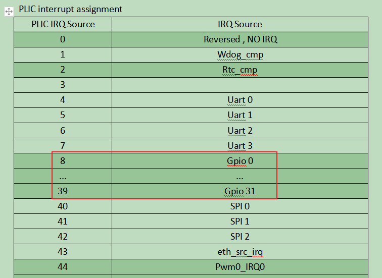
Figure 1 Interrupt source

Figure 2 GPIO interrupt source
2. Engineering code
2.1. platform.h
Note that the GPIO A group of the 2.02/2.03 version of the FII RISC-V CPU is connected to LEDs, the GPIO B and C groups are connected to digital tubes, and the GPIO D group is connected to buttons. When using the GPIO project, change the GPIO A group connection from the original LED to a DIP switch. Note that in addition to modifying the corresponding FPGA code, you also need to add the corresponding pin assignment. Figure 3 shows the modified GPIO A group wiring. Figure 4 shows the newly added pin assignments (the FII PRX100-D FPGA development board is used here, the detailed hardware reference guide is here ). Figure 5 shows the value and register direction of the GPIO register on the address map (click here for the detailed address map). In software engineering, the GPIO needs to be configured according to the corresponding address.

Figure 3 GPIO A group connection

Figure 4 DIP switch pin assignment
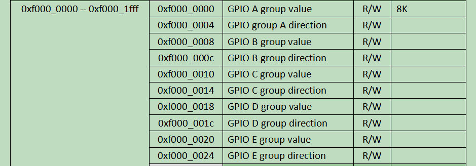
Figure 5 GPIO register address
//Define GPIO group offset

#define GPIO_A_GRP_IRQ_OFFSET (0)
#define GPIO_B_GRP_IRQ_OFFSET (8)
#define GPIO_C_GRP_IRQ_OFFSET (16)
#define GPIO_D_GRP_IRQ_OFFSET (24)

#define INT_GPIO_BASE 8 //Interrupt ID 8-39 is GPIO group

//bit 0-2 of GPIO D group is set as the interrupt source, the corresponding keys are menu, up, return

#define BUT_D_0 (0)
#define BUT_D_1 (1)
#define BUT_D_2 (2)

//The GPIO serial number corresponding to the three buttons

#define BUTTON_0_OFFSET (GPIO_D_GRP_IRQ_OFFSET + BUT_D_0)
#define BUTTON_1_OFFSET (GPIO_D_GRP_IRQ_OFFSET + BUT_D_1)
#define BUTTON_2_OFFSET (GPIO_D_GRP_IRQ_OFFSET + BUT_D_2)

//Interrupt ID corresponding to the three buttons

#define INT_DEVICE_BUTTON_0 (INT_GPIO_BASE + BUTTON_0_OFFSET)
#define INT_DEVICE_BUTTON_1 (INT_GPIO_BASE + BUTTON_1_OFFSET)
#define INT_DEVICE_BUTTON_2 (INT_GPIO_BASE + BUTTON_2_OFFSET)

//bits 5-7 of GPIO A group are set as the interrupt source, and the corresponding DIP switch is SW5-7

#define SW_5 (5)
#define SW_6 (6)
#define SW_7 (7)

//The GPIO serial number corresponding to the three DIP switches

#define SW_5_OFFSET (GPIO_A_GRP_IRQ_OFFSET + SW_5)
#define SW_6_OFFSET (GPIO_A_GRP_IRQ_OFFSET + SW_6)
#define SW_7_OFFSET (GPIO_A_GRP_IRQ_OFFSET + SW_7)

//Interrupt ID corresponding to the three DIP switches

#define INT_DEVICE_SW_5 (INT_GPIO_BASE + SW_5_OFFSET)
#define INT_DEVICE_SW_6 (INT_GPIO_BASE + SW_6_OFFSET)
#define INT_DEVICE_SW_7 (INT_GPIO_BASE + SW_7_OFFSET)
2.2. fii_gpio.h
Figure 6 shows the GPIO interrupt-related registers, taken from the address map (click here for the detailed address map ). A detailed explanation of the registers is shown in Figure 7.
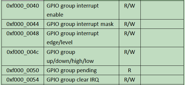
Figure 6 GPIO interrupt register
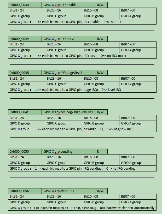
Figure 7 GPIO interrupt register explanation
#include "fii_types.h"

#define GPIO_ADDR (0xF0000000) //Define GPIO address range related parameters
#define GPIO_VAL (0x00) //The relative offset of the GPIO value
#define GPIO_DIR (0x04) // GPIO direction relative offset

//Define GPIO group

#define GPIO_A (0x00)
#define GPIO_B (0x08)
#define GPIO_C (0x10)
#define GPIO_D (0x18)

//Define the offset of the GPIO interrupt
#define GPIO_IRQ_GRP (0x40)

//Define the parameter offset related to GPIO interrupt

#define GPIO_IRQ_ENA (0x00) //Interrupt enable
#define GPIO_IRQ_MASK (0x04) //Interrupt mask
#define GPIO_IRQ_TRIGGER (0x08) //Interrupt edge/level
#define GPIO_IRQ_TYPE (0x0C) //Interrupt upper/lower edge or high/low voltage selection
#define GPIO_IRQ_PENDING (0x10) //Interrupt pending
#define GPIO_IRQ_CLR (0x14) //Interrupt clear


//Define GPIO related macros

//Define the direction of the GPIO pins

#define GPIO_SetBitDir(gpio_grp, gpio_bit, gpio_dir) ( \
    (gpio_dir == 0) ? (GPIO_REG(gpio_grp + 4) &= ~(1UL << gpio_bit)) \
                    : (GPIO_REG(gpio_grp + 4) |= 1UL << gpio_bit ) )

//Set GPIO bits
#define GPIO_SetBit(gpio_grp, gpio_bit) ( GPIO_REG( gpio_grp) |= 1UL << gpio_bit )

//Clear GPIO bits
#define GPIO_ClrBit(gpio_grp, gpio_bit) ( GPIO_REG( gpio_grp) &= ~(1UL << gpio_bit) )

//Read the bits of GPIO
#define GPIO_ReadBit(gpio_grp, gpio_bit) (( GPIO_REG(gpio_grp) >> gpio_bit ) & 0x01 )

// Aliases the GPIO related macros again
#define CPUPIN_DIR(ba,pin,d) GPIO_SetBitDir(ba,pin,d)
#define CPUPIN_SET(ba,pin) GPIO_SetBit(ba,pin)
#define CPUPIN_CLR(ba,pin) GPIO_ClrBit(ba,pin)
#define CPUPIN_GET(ba,pin) GPIO_ReadBit(ba,pin)

//Enumeration + aliasing to facilitate the use of GPIO interrupts later

typedef enum {
    GPIO_OUT = 0,
    GPIO_IN //default is 1
} E_GPIO_DIR;

typedef enum {
    GPIO_IRQ_DIS = 0,
    GPIO_IRQ_EN //default is 1
} E_GPIO_IRQ_SW;

typedef enum {
    IRQ_LEVEL = 0,
    IRQ_EDGE //default is 1
} E_IRQ_TRIGGER;

typedef enum {
    IRQ_NEG_LOW = 0,
    IRQ_POS_HIGH //default is 1
} E_IRQ_TYPE;

//Declare GPIO related functions, set the GPIO interrupt type, such as the edge or level that triggers the interrupt

void GPIO_IRQ_register( u32_t gpio_pin, E_GPIO_IRQ_SW gpio_sw,
E_IRQ_TRIGGER gpio_trigger, E_IRQ_TYPE gpio_type);