1. Introduction to I2C
Related reference articles:
RISC-V teaching plan
PRX100-D develops the EEPROM chip of AT24C02 onboard, and the test of the I2C bus is mainly the reading and writing of the device. Before entering the RISC-V I2C interrupt design, here is a brief introduction to the I2C bus.
I2C (Inter-Integrated Circuit) is a synchronous, multi-master, and multi-slave serial communication bus. It was originally invented by Philip and maintained by NXP Semiconductors. I2C is mainly used for communication between slow peripherals and processors in short distances within the board.
2. RISC-V I2C Design
Here, an I2C peripheral module is added on the basis of the original pipeline RISC-V CPU (version after V2.03) as an I2C0 module, and its interrupt i2c0_irq output is connected to the external platform-level interrupt processor for unified arbitration processing.
2.1. RISC-V I2C0 module design overview
- Standard Mode/Low-Speed Mode, the speed is less than or equal to 100 kbits/s
- Support byte writing, page (for AT24C02, the maximum page size is 8 bytes) writing
- Support current address read, random read (fake write, dummy write), sequential read
- Support Slave No Acknowledge Interrupt
- Support write data count error interrupt
- Support programmable read and write watermark interrupt
- The transfer rate can be controlled by writing the register DIV through software
The five read and write modes supported by RISC-V I2C0 are as follows:
-
Byte write
Figure 1 shows byte writing, that is, within a single operation (in the start and stop intervals), there is only one-byte data write operation. You can see that the host sends the device address + write bit, the host sends the register address, and the host sends one byte of data.

Figure 1 Byte write[1]
-
PageWrite
Figure 2 shows page writing. For AT24C02, page writing can write up to 8 bytes of data, and it needs to be an 8-byte aligned register address, that is, it can only be 0xX0 , 0xX8 register address (such as 0xe8 ) to start Write in the complete 8-byte data. According to the datasheet of AT24C02, if 8-byte data is written at an address that is not 8-byte aligned (or exceeds the length of the remaining aligned address), after the sequential writing, the data beyond the 8-byte aligned address is rolled back and overwritten to the alignment . the beginning of the address. For example, if 3 bytes of data (0x01, 0x02, 0x03) are written at the address of 0x07 , the final write operation is not 0x07–0x01 , 0x08–0x02 , 0x09-0x03 , but 0x07–0x01 , 0x00 –0x02, 0x01 -0x03. In the above example, 0x07 is at the aligned address 0x00-0x07middle. The reason why the write operation has this limitation is that the registers inside the AT24C02 will only increase by the lower three bits with the write operation (that is, the lower three bits of the register can only change from 3’b000 to 3’b111 during a single page write operation, In hexadecimal, the lowest bit can only be changed in the range of 0x0-0x7, 0x8-0xf in a single page write operation). This limitation can be solved by software-specific functions. In software, writing more than 8-byte, or writing more than the space left by the aligned address, is divided into page writes that AT24C02 can accept by software, and repeats until all the data are written. is written into EEPROM.

Figure 2 Page write[1]
-
current address read
The current address read is relatively simple. As shown in Figure 3, the host only sends the device address + read bit. In the case of not sending the register address, the register address of the last operation + 1, that is, the register read at the current address. After that, the slave sends one byte of data to the master.

Figure 3 Current address read[1]
-
random read
Figure 4 shows a random read operation, which includes a dummy write. The dummy write includes the host sending the device address + write bit, and the host sending the register address. After the fake write, the host resends the start bit and sends the device address + read bit. The slave replies to the master with one byte of data. Random read can be located to any address to read data through the pseudo-written register, so it is called “random read”.

Figure 4 Random read[1]
-
continuous reading
Continuous read can be extended from random read or current address read to multi-data byte read, as shown in Figure 5. As long as the master replies with ACK to the slave, the slave can always send data. If the register address is 0xff, the next address +1 will wrap around to the 0x00 register address to continue reading.
 Figure 5 Continuous read[1]
2.2. Address map
The register base address of I2C0 is 0xf000_4000, the detailed address map click here.
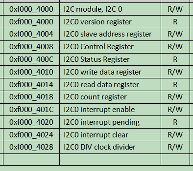
Figure 6 I2C0 register address
-
version register
Figure 7 shows the version register of the I2C0 module, which is only readable.
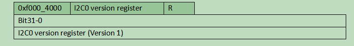
Figure 7 Version register
-
SLAVE address register
Figure 8 shows the slave address register, which is readable and writable. Bits 16-31 are reserved bits. Bits 15-8 are the slave’s register address, and bits 7-1 are the slave’s device address. Bit 0 indicates read/write operation, which is consistent with the I2C protocol, ‘0’ indicates write operation, and ‘1’ indicates read operation. The default value is 0x0000_00A0, that is, the default slave is AT24C02 (7’b1010_000), the default is write-operation, and the register address is 0x00.
Note: The register address of the slave is not necessary for the read operation. It is used in conjunction with the restart bit of the control register. If the restart bit stands up, it is a random read, otherwise it is the current address read.
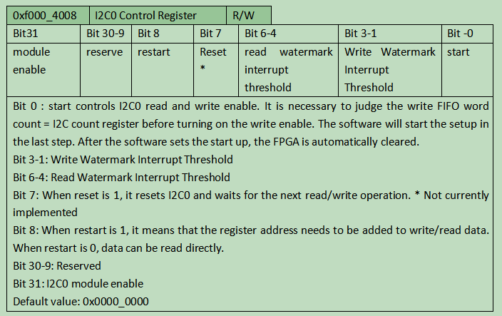
Figure 8 slave address register
-
control register
Figure 9 is the control register, which is readable and writable. Bit 31 is the enable of the entire I2C0 module, ‘1’ is enabled, ‘0’ is disabled. Bits 30-9 are temporarily reserved. Bit 8 is restart, ‘1’ indicates that the read/write operation needs to increase the register address (see slave address register bits 15-8), and ‘0’ indicates that the read operation does not use the register. Bit 7 is reset, which is not implemented at present and is temporarily reserved. Bits 6-4 are programmable read FIFO watermark thresholds, and bits 3-1 are programmable write FIFO watermark thresholds. Bit 0 is the start bit, which controls the I2C read and write enable. Before setting up the start bit, it is necessary to ensure that the word count in the write FIFO = the count in the I2C count register. If they are not equal, the write data count error interrupt may be caused. In software, the start bit is set in the last step. After the software sets the start bit up, the FPGA is automatically cleared. The default value is 0x0000_0000.
Figure 9 Control Register
-
status register
Figure 10 shows the status register, which is only readable. Bits 31-10 are reserved bits. Bits 9-6 are the word count output from the read FIFO. bit 5 is read FIFO empty. Bit 4-1 is the word count output by the write FIFO. bit 0 is write FIFO full.
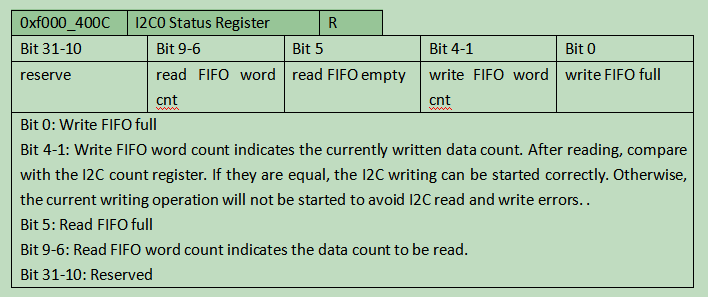
Figure 10 Status Register
-
write data register
Figure 11 shows the write data register, which can be read and written. Bits 31-8 are reserved bits. Bits 7-0 are write data, with 8 bits/byte as the minimum unit. The default value is 0x0000_0000.
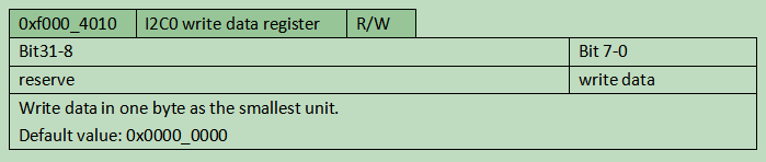
Figure 11 Write data register
-
read data register
Figure 12 is the read data register, only readable. Bits 31-8 are reserved bits. Bits 7-0 are read data, and the minimum unit is 8 bits/byte.
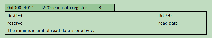
Figure 12 Read data register
-
count register
Figure 13 is the count register, which is readable and writable. Programmable, the maximum value is 15 bytes of data. Before the start bit of the control register is set up, it is necessary to ensure that the word count output by the write FIFO is equal to the value in the count register. If they are not equal, the write data count error may be interrupted.
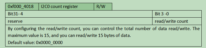
Figure 13 Count register
-
Interrupt Enable, Suspend and Clear
Figure 14 shows the interrupt enable, hang and clear registers. The interrupt pending register is readable only, and the interrupt enable and clear registers are readable and writable. RISC-V I2C0 supports 4 kinds of interrupts: read watermark interrupt, write watermark interrupt, no acknowledge interrupt and write data count error interrupt. Bits 31-4 of the Interrupt Enable, Suspend and Clear registers are reserved. Bit 3 of the interrupt register is a write data count error interrupt, bit 2 corresponds to a no-response interrupt, bit 1 is a watermark read interrupt, and bit 0 is a watermark write interrupt.
When the word count output by the write FIFO is not equal to the value in the count register (for example, the I2C0 count register is configured as 8 bytes, but the data written to the FIFO is only 7 bytes), derror is set up. When the slave does not respond and does not send an ACK, the nack is set up. When the data in the read FIFO is strictly greater than the threshold in the read watermark of the control register, rwm is set up. When the data is less than the threshold, the corresponding dangling bit is cleared. When the data in the write FIFO is strictly less than the threshold in the write watermark of the control register, wwm is set up. When the data exceeds the threshold, the corresponding dangling bit is cleared. After the software sets up the interrupt clear bit, the hardware will automatically clear it to zero to ensure that the software writes to the interrupt clear register once only corresponding to clearing the interrupt suspension once.
Both the interrupt enable and clear registers have default values of 0x0000_0000.
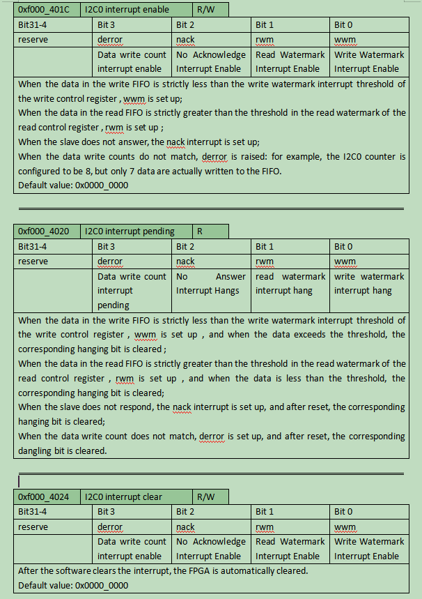
Figure 14 Interrupt Enable, Suspend and Clear Registers
-
Div Clock Divide
The clock divider register is shown in Figure 15. Div is calculated as (f in / F) – 1. f in is the main frequency of the system clock of the FPGA, and F is the target transmission frequency. Bits 31-16 in the DIV register are reserved bits, and bits 15-0 are the actual written divider. Taking the 100 kbits/s transmission rate and 50 MHz main frequency used here as an example, the calculated result of DIV is 499 (100k = 50M/(DIV + 1), DIV = 499). The default value of the clock divider register is 0x0000_2000 (the calculated target transmission frequency is much less than 100 kbits/s).
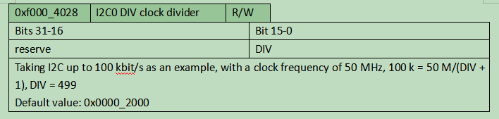
Figure 15 Clock divider register
3. Article references
[1] Ww1.microchip.com , 2021. [Online]. Available: http://ww1.microchip.com/downloads/en/DeviceDoc/Atmel-8871F-SEEPROM-AT24C01D-02D-Datasheet.pdf. [Accessed: 19-May-2021].