1. Introduction to UART
Related reference articles:
RISC-V teaching plan
Before entering the RISC-V UART interrupt design, here is a brief introduction to the UART. UART (universal asynchronous receiver-transmitter), universal asynchronous serial transceiver. The UART receives the data bytes and transmits the individual bits in a sequential fashion, and another UART at the destination reassembles the bits into complete bytes. UART converts parallel data to the serial transceiver, communication can be simplex (only in one direction, there is no requirement for the receiving device to send information back to the sending device), full-duplex (two devices transmit and receive at the same time) or half-duplex. Duplex (devices take turns sending and receiving).
2. RISC-V UART design
The RISC-V CPU has previously implemented a UART for transmitting instructions to ITCM. Here is a new UART module, UART1, for the implementation and application of external platform-level interrupts.
2.1. RISC-V UART1 design overview:
- 8-bit data + optional parity bit + optional 1/2 stop bit
- The parity check bit options are no check, odd check (odd), even check (even), 1 check (mark), 0 check (space)
- Watermark interrupt supporting programmable transmit and receive FIFO
- Support check bit error interrupt
- The register DIV can be written by software to control the baud rate
2.2. Address map
The register address of UART1 is arranged after the previous UART register, with 0xe000_1000 as the base address (click here for the detailed address map ).
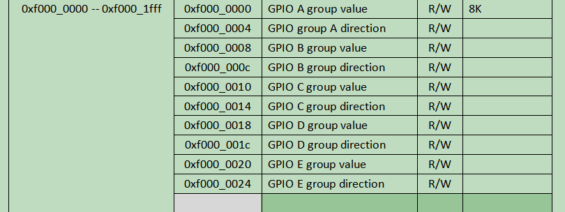
Figure 1 UART1 register address
-
TXDADA, transmit data register
The UART1 transmit data register is shown in Figure 2, in which the transmitted data is bit 0-7, and bit 31 is the FIFO transmission full flag. That is to say, if bit 31 of TXDATA is 0, it means that the transmit FIFO is not full, and the transmit data can continue to be written; on the contrary, if bit 31 of TXDATA is 1, it means that the transmit FIFO is full and no more data can be written. TXDATA bits 8-30 are currently reserved. If the transmit FIFO is not full, the transmit data in TXDATA will directly enter the FIFO after being written by software.
Although TXDATA is a readable and writable register (R/W stands for read/write), when reading the TXDATA register, only the FIFO full flag can be read, and the value of bit 0-7 of the transmitted data is 0. If the read value of the FIFO full flag is 1, the write transmit data bit is ignored.
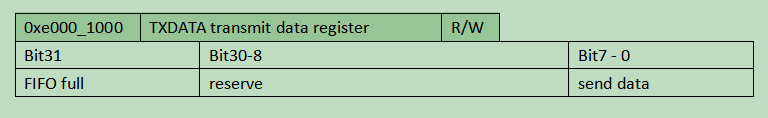
Figure 2 Transmit data register
-
RXDADA, Receive Data Register
The UART1 receive data register is shown in Figure 3. Similar to the transmit register, bits 0-7 are received data, bit 31 is the FIFO empty flag, and the rest of the bits are temporarily reserved. RXDATA is a read-only register. When bit 31 of RXDATA is 1, it means that the receive FIFO is empty, that is, there is no data to read. When bit31 of RXDATA is 0, the received data can be read normally.
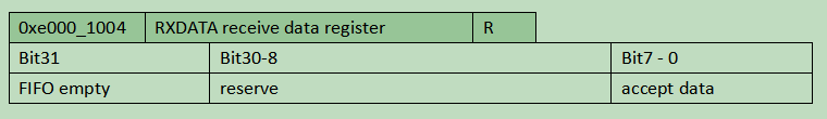
Figure 3 Receive data register
-
TXCTRL, transmit control register
The UART1 transmission control register is shown in Figure 4, bit 0 is the transmission enable, bit 1 controls the number of stop bits, 0 corresponds to one stop bit, and 1 corresponds to two stop bits. Bits 16-18 are the interrupt threshold for sending FIFO watermarks. Other bits of TXCTRL are reserved.
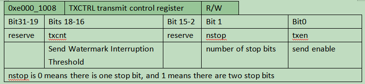
Figure 4 Send Control Register
-
RXCTRL, Receive Control Register
The UART1 receiving control register is shown in Figure 5, bit 0 is the receiving enable, and bits 16-18 are the interrupt threshold of the receiving FIFO watermark. Other bits of RXCTRL are reserved.
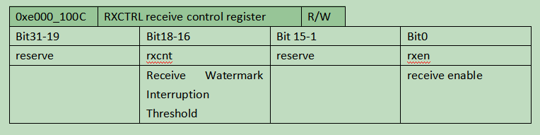
Figure 5 Receive Control Register
-
IE, IP and IC, Interrupt Enable, Interrupt Pending and Interrupt Clear
The UART1 interrupt enable, interrupt pending and interrupt clear registers are shown in Figure 6. The IE register and IC register of RISC-V UART1 are both readable and writable, and the IP register is only readable. RISC-V UART1 supports 3 kinds of interrupts: parity check interrupt, receive watermark interrupt and transmit watermark interrupt. Bit 0 of IE, IP and IC correspond to sending watermark interrupt, bit 1 corresponds to receiving watermark interrupt, and bit 3 corresponds to parity check interrupt. When there is an error in the parity check, perror is raised; when the data in the transmit FIFO is strictly less than the threshold in the txcnt of the txctrl register, txwm is raised. When the data exceeds the threshold, the corresponding hanging bit is cleared; when the data in the transmit FIFO is strictly greater than the threshold in the rxcnt of the rxctrl register, rxwm is set up. When the data is less than the threshold, the corresponding dangling bit is cleared. After the software stands up the interrupt clearing IC, the hardware will automatically clear it to zero, ensuring that the software writes to the interrupt clearing register once only corresponds to clearing the interrupt suspension once.
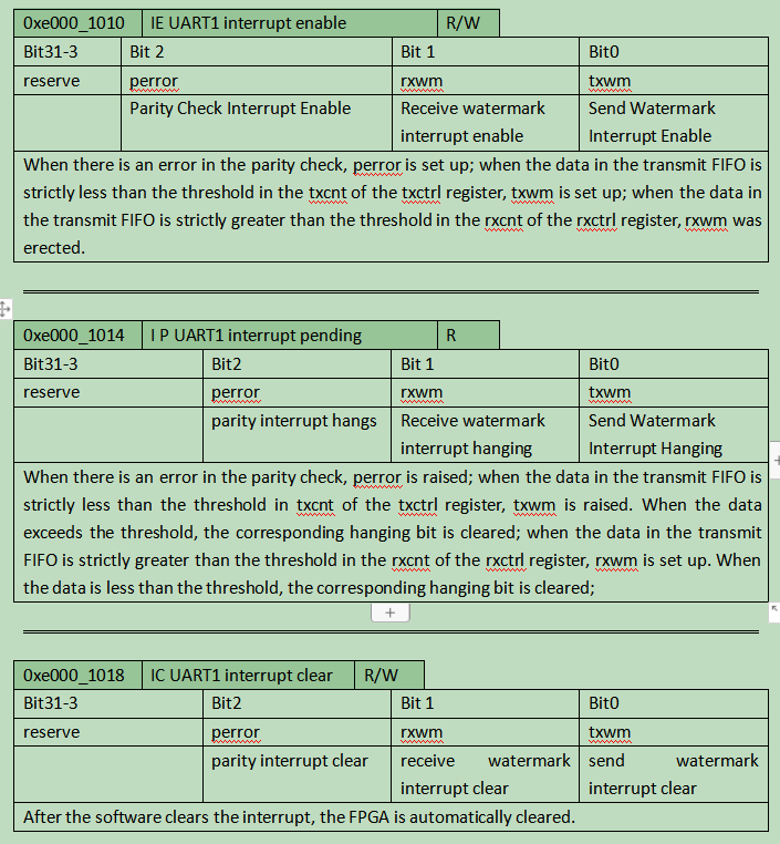
Figure 6 Interrupt Enable, Interrupt Pending and Interrupt Clear Registers
-
DIV, Baud Rate Divider Register
The UART1 baud rate divider register is shown in Figure 7. f in is the main frequency of the system clock of the FPGA, and bits 0-15 in the DIV register are the actual written baud rate division divisors. Bits 16-31 are reserved bits. Div is calculated as (f in / F baud ) – 1. Taking some common baud rates as an example, taking the main frequency of 50 MHz as an example, Figure 8 is the corresponding div value calculated.
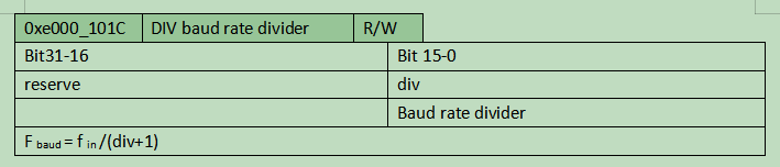
Figure 7 Baud rate divider register

Figure 8 Take the common baud rate as an example, its corresponding div value
-
LCR, Parity Check Register
The parity check register of UART1 is shown in Figure 9. The LCR register is compatible with the UART LCR register of TI (Texas Instrument) and Texas Instruments, so a similar definition is used. Only the parity check used for bit 3-5 selection is used here, and the rest of the bits are temporarily reserved. The bit 3-5 of the LCR select the parity check method as shown in Figure 9. For example, if even check is selected, it can be seen from the table in Figure 9 that LCR[5:3] needs to be set to 3’b011.
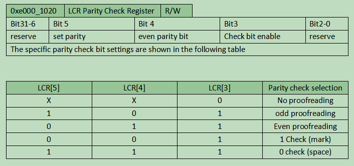
Figure 9 LCR Parity Check Register