1. Read the timer interrupt register
Related reference articles:
RISC-V teaching plan
The exu_lsu module was introduced in the RISC-V LSU, SRAM, GPIO module (1) exu_lsu module before, which allows the RISC-V CPU to access the peripheral module. This article will introduce the submodule fii_timer_lsu under the exu_lsu module that was not mentioned before.

First, refer to the register definition related to timer interrupt on the FII RISC-V Address Map , as shown in Figure 1. It can be seen that there are timer control registers, low 32-bit and high 32-bit registers for timer values, and low 32-bit and high 32-bit registers for timer comparison values. The relevant read (load) code is in the exu_lsu module, see the following code:
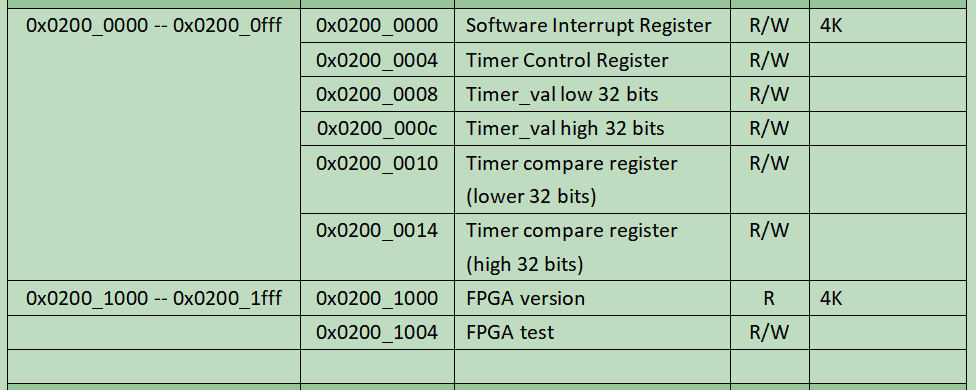
Figure 1 Timer Interrupt Register
parameter [ 31: 0 ] TMR_BASEADDR = 32'h0200_0000//Timer interrupt register base address parameter
wire t_sft_cs   = ( i_D_PC[ 31: 16 ] == TMR_BASEADDR[ 31: 16 ] ) ? 1'b1 : 1'b0;//Timer related register chip select
wire sft_cs     = t_sft_cs & ( ( ~i_D_PC[ 12 ] ) & ( i_D_PC[ 5: 2 ] == 0 ) );
wire tm_ctrl_cs = t_sft_cs & ( ( ~i_D_PC[ 12 ] ) & ( i_D_PC[ 5: 2 ] == 1 ) );//timer control register chip select
wire t_cs0      = t_sft_cs & ( ( ~i_D_PC[ 12 ] ) & ( i_D_PC[ 5: 2 ] == 2 ) );//low 32-bit register chip select of timer value
wire t_cs1      = t_sft_cs & ( ( ~i_D_PC[ 12 ] ) & ( i_D_PC[ 5: 2 ] == 3 ) );//high 32-bit register chip select of timer value
wire tcmp_cs0   = t_sft_cs & ( ( ~i_D_PC[ 12 ] ) & ( i_D_PC[ 5: 2 ] == 4 ) );//Lower 32-bit register chip select of timer compare value
wire tcmp_cs1   = t_sft_cs & ( ( ~i_D_PC[ 12 ] ) & ( i_D_PC[ 5: 2 ] == 5 ) );//high 32-bit register chip select of timer compare value

//According to the chip select signal, determine the register to be read
wire [ 31: 0 ] ls_rb_d_t_sft = sft_cs     ? o_sft_int_v :
                             ( tm_ctrl_cs ? o_tm_ctrl :
                                  ( t_cs0 ? i_timer_l :
                                  ( t_cs1 ? i_timer_h :
                               ( tcmp_cs0 ? o_tcmp_l :
                               ( tcmp_cs1 ? o_tcmp_h : o_CPU_dout ) ) ) ) );

//According to the chip select signal, determine the register to be read
wire [ 31: 0 ] ls_rb_d = mem_cs ? mem_dout : ( GPIO_cs ? rb_GPIO_d : ( UART_cs ? o_UART_dout : ls_rb_d_t_sft ) );


always@( * )//part of the code block is omitted
begin
if ( i_LOAD )
begin //&mem_init_rdy
    case ( i_load_instr ) // i_load_instr ={rv32i_lbu, rv32i_lb, rv32i_lhu, rv32i_lh, rv32i_lw};
    5'b00001:
    begin //rv32i_lw
        o_wb_data <= ls_rb_d;
    end
    5'b00010:
    begin //rv32i_lh
        o_wb_data <= { { 16{ ls_rb_d[ 15 ] } }, ls_rb_d[ 15: 0 ] };
    end
    5'b00100:
    begin //rv32i_lhu
        o_wb_data <= { { 16{ 1'b0 } }, ls_rb_d[ 15: 0 ] };
    end
    5'b01000:
    begin //rv32i_lb
        o_wb_data <= { { 24{ ls_rb_d[ 7 ] } }, ls_rb_d[ 7: 0 ] };
    end
    5'b10000:
    begin //rv32i_lbu
        o_wb_data <= { { 24{ 1'b0 } }, ls_rb_d[ 7: 0 ] };
    end
default: ;

endcase
end
2. Write the timer interrupt register
The write (store) of the timer interrupt register is done in the fii_timer_lsu module. The corresponding register to be written is selected through the write enable signal introduced from the outer module exu_lsu, as well as various chip select signals. code show as below:
wire [31: 0] cpu_data_in = i_rs2_val << {i_D_PC[1:0],3'b000};//The cpu_data_in in the exu_lsu module is finally passed to i_sft_timer_din

always@( posedge clk or negedge rst_n )
if ( !rst_n )//reset
begin
    o_tm_ctrl <= 0;//initial value
    o_sft_int_v <= 0;
    o_timer_l <= 0;
    o_timer_h <= 0;
    o_tcmp_l <= 0;
    o_tcmp_h <= 16'h8000;
    o_timer_valid <= 0;
end
else
begin
    o_timer_valid <= 0;

    if ( i_tmr_sft_we )//write enable signal
    begin
        if ( i_tcs0 )//The low 32-bit register chip select of the timer value
        begin
            o_timer_l <= i_sft_timer_din;//Write into the lower 32-bit register of the timer value
            o_timer_valid[ 0 ] <= 1'b1;
        end

        if ( i_tcs1 )//The high 32-bit register chip select of the timer value
        begin
            o_timer_h <= i_sft_timer_din;//Write into the upper 32-bit register of the timer value
            o_timer_valid[ 1 ] <= 1'b1;
        end

        if ( i_tcmp_cs0 )//The low 32-bit register chip select of the timer comparison value
            o_tcmp_l <= i_sft_timer_din;//Write into the lower 32-bit register of the timer comparison value

        if ( i_tcmp_cs1 )//The high 32-bit register chip select of the timer comparison value
            o_tcmp_h <= i_sft_timer_din;//Write into the upper 32-bit register of the timer comparison value

        if ( i_tm_ctrl_cs )//Timer control register chip select
            o_tm_ctrl <= i_sft_timer_din;//Write into the timer control register
    end
end