The LOAD and STORE instructions in the RISC-V CPU control the SRAM and GPIO modules, SRAM, GPIO, etc., can be regarded as the external storage of the cpu. In the Harvard architecture, use the data bus to access these external modules
Related reference articles:
RISC-V teaching plan
GPIO address space:
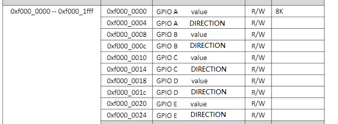
The gpio register address space is an 8k address space starting at 0xf000_0000.

gpio module code:
module fii_GPIO
#(
    parameter GPIO_DEEP   = 8,  //memory data width
    parameter GPIO_W      = 32, //memory data width
    parameter GPIO_MSK_W  = 4,  //memory data mask width
    parameter GPIO_ADDR_W = 32  //memory address width
)
(
    input clk,                                // system clock
    input rst_n,

    input [ GPIO_W - 1 : 0 ] i_ls_GPIO_din,   // cpu write data
    output [ GPIO_W - 1 : 0 ] o_rb_GPIO_dout, // cpu read data

    input [ GPIO_ADDR_W - 1 : 0 ] i_addr,     // data bus address
    input i_cs,                               // gpio module chip select
    input i_we,                               // write signal
    input [ GPIO_MSK_W - 1: 0 ] i_wem,        // write mask signal

    // t = 0, output; t = 1, input
    input [ 31: 0 ] i_GPIO_dina,              // GPIO module a group cpu write data
    output [ 31: 0 ] o_GPIO_douta,            // GPIO module a group cpu read data
    output [ 31: 0 ] o_GPIO_ta,               // direction control of gpio module a group

    input [ 31: 0 ] i_GPIO_dinb,              // GPIO module b group cpu write data
    output [ 31: 0 ] o_GPIO_doutb,            // GPIO module b group cpu read data
    output [ 31: 0 ] o_GPIO_tb,               // direction control of gpio module b group

    input [ 31: 0 ] i_GPIO_dinc,              // GPIO module c group cpu write data
    output [ 31: 0 ] o_GPIO_doutc,            // GPIO module c group cpu read data
    output [ 31: 0 ] o_GPIO_tc,               // direction control of gpio module c group

    input [ 31: 0 ] i_GPIO_dind,              // GPIO module d group cpu write data
    output [ 31: 0 ] o_GPIO_doutd,            // GPIO module d group cpu read data
    output [ 31: 0 ] o_GPIO_td                // direction control of gpio module d group
);
//===============================================================================
reg [ GPIO_W - 1: 0 ] GPIO_r [ 0: GPIO_DEEP - 1 ];
wire [ GPIO_MSK_W - 1: 0 ] wen;
wire ren;
wire [ 2: 0 ] w_addr = i_addr[ 4: 2 ];

//===============================================================================
assign ren = i_cs & ( ~i_we );
assign wen = ( { GPIO_MSK_W{ i_cs & i_we } } & i_wem );

reg [ GPIO_ADDR_W - 1: 0 ] addr_r = 0;
always@( posedge clk )
if ( ren )
    addr_r <= i_addr;

//===============================================================================
reg [7:0] i = 0;
initial
begin
    for ( i = 0; i < GPIO_DEEP; i = i + 1 )
    begin:IO_GPIO_INIT
        GPIO_r <= ~0;
    end
end

genvar wi;
generate
    for ( wi = 0; wi < GPIO_MSK_W; wi = wi + 1 )
    begin:IO_write
        always @( posedge clk )
        begin
           if ( wen[ wi ] )
           begin
               GPIO_r[ w_addr ][ 8 * wi + 7: 8 * wi ] <= i_ls_GPIO_din[ 8 * wi + 7: 8 * wi ];
           end
        end
    end
endgenerate
//===============================================================================
wire [ GPIO_W - 1: 0 ] dout_pre;
wire [ GPIO_W - 1: 0 ] t_pre;
wire [ GPIO_W - 1: 0 ] reg_dout;
wire [ GPIO_W - 1: 0 ] in_dout[ 0: GPIO_DEEP / 2 - 1 ];

assign in_dout[ 0 ] = i_GPIO_dina;
assign in_dout[ 1 ] = i_GPIO_dinb;
assign in_dout[ 2 ] = i_GPIO_dinc;
assign in_dout[ 3 ] = i_GPIO_dind;

//wire [ 31: 0 ] in_dout_tmp = in_dout[ i_addr[ GPIO_DEEP / 2 - 1: 1 ] ];
wire [ 31: 0 ] in_dout_tmp = in_dout[ w_addr[ 2: 1 ]];


//assign t_pre = GPIO_r[ { addr_r[ GPIO_ADDR_W - 1: 1 ], 1'b1 } ];
//assign dout_pre = GPIO_r[ { addr_r[ GPIO_ADDR_W - 1: 1 ], 1'b0 } ];
assign t_pre    = GPIO_r[ { w_addr[ 2: 1 ], 1'b1 } ];
assign dout_pre = GPIO_r[ { w_addr[ 2: 1 ], 1'b0 } ];

//===============================================================================
genvar rbi;
generate
    for ( rbi = 0; rbi < GPIO_W; rbi = rbi + 1 )
    begin:GPIO_readb
    // input reg output reg
        assign o_rb_GPIO_dout[ rbi ] = t_pre[ rbi ] ? in_dout_tmp[ rbi ] : dout_pre[ rbi ];
    end
endgenerate
//===============================================================================
assign o_GPIO_douta = GPIO_r[ 0 ];
assign o_GPIO_ta    = GPIO_r[ 1 ];

assign o_GPIO_doutb = GPIO_r[ 2 ];
assign o_GPIO_tb    = GPIO_r[ 3 ];

assign o_GPIO_doutc = GPIO_r[ 4 ];
assign o_GPIO_tc    = GPIO_r[ 5 ];

assign o_GPIO_doutd = GPIO_r[ 6 ];
assign o_GPIO_td    = GPIO_r[ 7 ];
//===============================================================================

endmodule
Port introduction:
input [ GPIO_W – 1 : 0 ] i_ls_GPIO_din , // cpu write data
output [ GPIO_W – 1 : 0 ] o_rb_GPIO_dout , // cpu read data
input [ GPIO_ADDR_W – 1 : 0 ] i_addr , // data bus address
input i_cs , // gpio module chip select
input i_we , // write signal
input [ GPIO_MSK_W – 1: 0 ] i_wem , // write mask signal
input [ 31: 0 ] i_GPIO_dina , // GPIO module a group cpu write data
output [ 31: 0 ] o_GPIO_douta , // gpio module a group cpu read data
output [ 31: 0 ] o_GPIO_ta , // gpio module a group a direction control
input [ 31: 0 ] i_GPIO_dinb , // gpio module b group cpu write data
output [ 31: 0 ] o_GPIO_doutb , // gpio module b group b cpu read data
output [ 31: 0 ] o_GPIO_tb , // gpio module b group direction control
input [ 31: 0 ] i_GPIO_dinc , // gpio module c group cpu write data
output [ 31: 0 ] o_GPIO_doutc , // gpio module c group c cpu read data
output [ 31: 0 ] o_GPIO_tc , // gpio module c group direction control
input [ 31: 0 ] i_GPIO_dind , // gpio module d group cpu write data
output [ 31: 0 ] o_GPIO_doutd , // gpio module d group cpu read data
output [ 31: 0 ] o_GPIO_td // gpio module d group direction control
Define the gpio register set:
reg [ GPIO_W – 1: 0 ] GPIO_r [ 0: GPIO_DEEP – 1 ];
Define read, write, address signals:
wire [ GPIO_MSK_W – 1: 0 ] wen;
wire ren;
wire [ 2: 0 ] w_addr = i_addr[ 4: 2 ];
assign ren = i_cs & ( ~i_we );
assign wen = ( { GPIO_MSK_W{ i_cs & i_we } } & i_wem );
gpio module register set, write logic:
genvar wi;
generate
    for (wi = 0; wi < GPIO_MSK_W; wi = wi + 1 )
    begin:IO_write
        always @( posedge clk )
        begin
            if ( wen[ wi ] )
            begin
                GPIO_r[ w_addr ][ 8 * wi + 7: 8 * wi ] <= i_ls_GPIO_din[ 8 * wi + 7: 8 * wi ];
            end
        end
    end
endgenerate
Read the direction register, data register in the gpio group:
wire [ GPIO_W - 1: 0 ] dout_pre;
wire [ GPIO_W - 1: 0 ] t_pre;
wire [ GPIO_W - 1: 0 ] reg_dout;
wire [ GPIO_W - 1: 0 ] in_dout[ 0: GPIO_DEEP / 2 - 1 ];

assign in_dout[ 0 ] = i_GPIO_dina;
assign in_dout[ 1 ] = i_GPIO_dinb;
assign in_dout[ 2 ] = i_GPIO_dinc;
assign in_dout[ 3 ] = i_GPIO_dind;

wire[ 31: 0 ] in_dout_tmp = in_dout[ w_addr[ 2: 1 ]];


assign t_pre = GPIO_r[ { w_addr[ 2: 1 ], 1'b1 } ]; // GPIO selected by current address, direction register in group A, B, C, D
assign dout_pre = GPIO_r[ { w_addr[ 2: 1 ], 1'b0 } ]; // Read the gpio value register in the GPIO, A, B, C, D group selected by the current address
The cpu writes the gpio register set:
genvar wi;
generate
    for (wi = 0; wi < GPIO_MSK_W; wi = wi + 1 )
    begin:IO_write
        always @( posedge clk )
        begin
            if ( wen[ wi ] )
            begin
                GPIO_r[ w_addr ][ 8 * wi + 7: 8 * wi ] <= i_ls_GPIO_din[ 8 * wi + 7: 8 * wi ];
            end
        end
    end
endgenerate
The cpu reads the contents of the gpio register set:
genvar rbi;
generate
    for( rbi = 0; rbi < GPIO_W; rbi = rbi + 1 )
    begin:GPIO_readb
    // input reg output reg
        assign o_rb_GPIO_dout[ rbi ] = t_pre[ rbi ] ? in_dout_tmp[ rbi ] : dout_pre[ rbi ];
    end
endgenerate
When t_pre == 1, read the value of the input fpga pin; when t_pre == 0, read the value in the current gpio value register;

Output the contents of the gpio register file to the primitives in the top-level file:
assign o_GPIO_douta = GPIO_r[ 0 ];
assign o_GPIO_ta = GPIO_r[ 1 ];
assign o_GPIO_doutb = GPIO_r[ 2 ];
assign o_GPIO_tb = GPIO_r[ 3 ];
assign o_GPIO_doutc = GPIO_r[ 4 ];
assign o_GPIO_tc = GPIO_r[ 5 ];
assign o_GPIO_doutd = GPIO_r[ 6 ];
assign o_GPIO_td = GPIO_r[ 7 ];