When the entire RISC-V kernel module is completed, the ITCM module is required to read the machine code of the code written by the software, and execute the current machine code according to logic such as instruction fetch, decoding, execution, memory access, and write back. These 5 parts It is not sent every time, and sometimes returns early, such as addi, without accessing external memory. In versions of RISC-V V3.00 and later, the pipeline method is used to process cpu instructions. We use a 3-stage pipeline method.
Related reference articles:
RISC-V teaching plan
Pipeline block diagram:
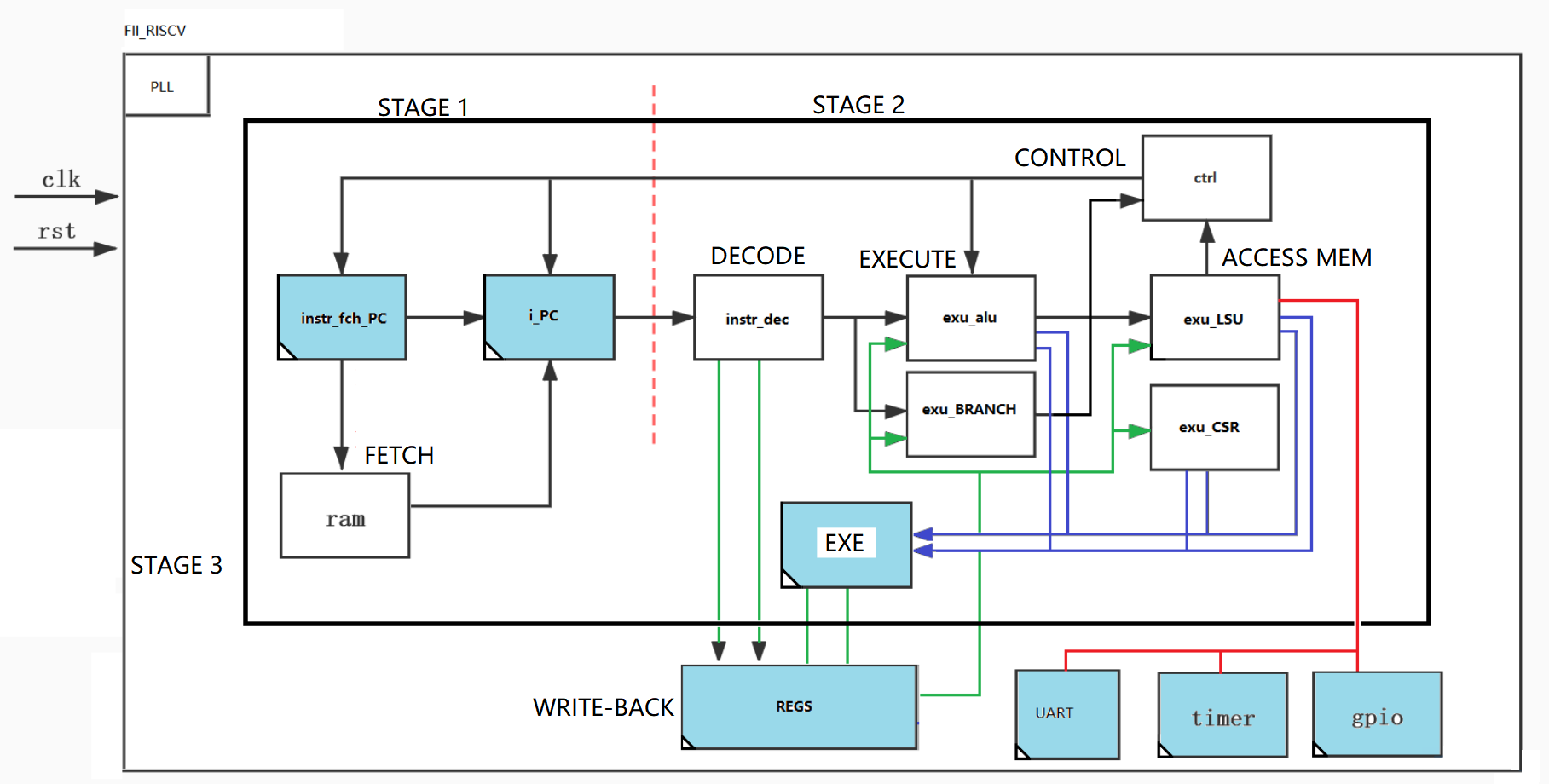
The blue squares in the figure are all D flip-flop latches. Represents the level of the pipeline.
First stage pipeline:
Since we use dual-port memory as ITCM (instruction memory), after each address is given, we need to wait for one clock cycle before we can get the corresponding instruction data. So the process of fetching takes 2 clock cycles. But this part still belongs to the first-level pipeline category (instruction fetch). If you use reg to accumulate a ram, it will save one clock cycle, but the disadvantage is that it takes up a lot of FPGA system resources.
Second stage pipeline:
Process the entire decoding, and execution stage. Including decoder (decoding), ALU (execution), branch (branch instruction execution), CSR (register related execution)
The third stage pipeline:
Writes back 32 general-purpose registers (regfile). If it is a LOAD/STORE-related instruction, handle peripheral-related operations. This part will be connected to the bus, including gpio, timer, Uart, and peripherals required for RISC-V cpu expansion later.
The cpu instruction fetch module pipeline:
`timescale 1ns / 1ps

module fii_instr_rib
# (
    parameter [31:0] DBG_BASEADDR  = 32'h0000_0800,
    parameter [31:0] TMR_BASEADDR  = 32'h0200_0000,
    parameter [31:0] PLIC_BASEADDR = 32'h0c00_0000,
    parameter [31:0] CPU_BASEADDR  = 32'h8000_0000,
    parameter [31:0] MEM_BASEADDR  = 32'h9000_0000,
    parameter [31:0] UART_BASEADDR = 32'he000_0000,
    parameter [31:0] PWM_BASEADDR  = 32'hf000_2000,
    parameter [31:0] GPIO_BASEADDR = 32'hf000_0000
)
(
    input  sys_clk,

    output reg [31:0] o_curr_pc,
    output [31:0]   o_curr_instr,

//===============================================================================
    input           i_pc_chg_flag,
    input           i_ir_hold_flag,
    input  [31:0]   i_exe_next_PC,

    output          o_CPU_load_vld,
//===============================================================================

    input  i_ext_irq,
    input  i_sft_irq,
    input  i_tmr_irq,

    input  o_glb_irq,                 // mstatus[3]; enable all Machine Mode interrupt

    input  [31:0] i_dbg_entry_adr,    // jtag debug entry address
    input  i_dbg_entry_set,           // jtag debug entry address enable ( one clock )

    input  [31:0] i_dpc_r,
    input  [31:0] i_dbg_instr,
    input  dret,

    input  [31:0]  i_mepc,
    input  [31:0]  i_vect_pc,                    // mtvec regitesr content
    output o_irq_src,
    output o_exp_src,
    input  mret,
    input  dbg_start,

//===============================================================================
    input  itcm_wea,
    input  [31:0] itcm_addra,
    input  [31:0] itcm_dina,

//===============================================================================
    input  [31:0] i_rib_saddr,
    input  [31:0] i_rib_sdin,
    output [31:0] o_rib_sdout,
    input  i_rib_svalid,
    output [1:0] o_rib_sready,
    input  [3:0]  i_rib_swe,
    input  i_rib_srd,
    input  i_rib_sop,
//===============================================================================
    // master bus signal
    input  i_rib_mvalid,
    input  [1:0] i_rib_mready,
//===============================================================================

    input  i_cpu_reset,
    input  rst_n
);

//===============================================================================
// cpu master bus operation

// long instruction : dec_instr should be set as 'INST_NOP, during long instruction.
reg  rib_delay_op = 0;
always @ ( posedge sys_clk or negedge rst_n)
if(!rst_n) rib_delay_op <= 0;
//else if ( o_rib_mvalid & ~i_rib_mready[0] ) rib_delay_op <= 1;
else if ( i_rib_mvalid ^ i_rib_mready[0] ) rib_delay_op <= 1;
else rib_delay_op <= 0;


wire  bus_hsk_ok = i_rib_mvalid & i_rib_mready[0];

// long period load & store operation; normal operation long_ir_flag is 0
wire  long_ir_flag = ( i_rib_mvalid & (~i_rib_mready[0]) ) | rib_delay_op;

// long period instruction pos edge; normal operation long_ir_cs is 0
wire  long_ir_cs = ( i_rib_mvalid & (~i_rib_mready[0]) ) & i_rib_sop;

//===============================================================================
wire o_CPU_load_cs = ( i_rib_saddr[ 31: 16 ] == CPU_BASEADDR[ 31: 16 ] ) ? i_rib_sop : 1'b0;
/*
ls_r is used for 0x8000_0000 DATA load instruction, becasue 0x8000_0000 is dual
port ram , it will be delay 2 clock (output data form dual port ram), the ls_r[1]
is signal that o_cpu_load_cs delay 2 clock
*/


reg [1:0] ls_r = 0;
always @( posedge sys_clk or negedge rst_n)
if(!rst_n) ls_r <= 0;
else
    ls_r <= {ls_r[0], o_CPU_load_cs};


assign o_CPU_load_vld = ls_r[1];
assign o_rib_sready = {1'b0, ls_r[1]};
//===============================================================================
wire [31:0] pc_instr;

wire [31:0] i_CPU_load_data = pc_instr;

wire [ 4: 0 ] data_sft = {i_rib_saddr[ 1: 0 ], 3'b000};  //i_D_PC[ 1: 0 ] * 8;
wire [ 31: 0 ] o_CPU_dout = i_CPU_load_data >> data_sft;

assign o_rib_sdout = o_CPU_dout;

//===============================================================================
reg [ 31: 0 ] instr_fch_PC = 0;
//===============================================================================

/*
next_addr is relevent o_cpu_load_cs, for example : current program pc is 0x8000_0004,
(load instruction ,data at 0x8000_01000), next_addr will be next program pc
0x8000_0004 + 4, after load instruction finish.
*/

reg [31:0] next_addr = 0;
always @( posedge sys_clk )
if(!rst_n | i_cpu_reset) next_addr <= CPU_BASEADDR;
else if(i_rib_sop) next_addr <= instr_fch_PC;
//===============================================================================
assign o_exp_src = 0;
wire nop_flag;
// don't generate interrupt when cpu load & flush instruction
assign o_irq_src = (long_ir_flag | nop_flag) ? 1'b0 : (i_ext_irq | i_sft_irq | i_tmr_irq);

wire irq_exp_flag = (o_irq_src & o_glb_irq) | o_exp_src ;  // edge o_irq_src high, then o_glb_irq low
//===============================================================================
reg  [31:0] jump_addr = 0;
always @( * )
begin
    if(i_dbg_entry_set)
        jump_addr = i_dbg_entry_adr;
    else if(dret)
        jump_addr = i_dpc_r;
    else if (long_ir_cs) // long address & (addr == 0x8000_xxxx)
        jump_addr = {i_rib_saddr[31:2], 2'b00};
    else if( irq_exp_flag )
        jump_addr = i_vect_pc;    // mtvec regitesr content
    else if( mret )
        jump_addr = i_mepc;       // The PC before enter interrupt
    else if( i_ir_hold_flag )
        jump_addr = o_curr_pc;    // long term instruction ,pc hold at current position
    else jump_addr = i_exe_next_PC;
end

wire w_jump_flag = i_dbg_entry_set | dret | irq_exp_flag | i_pc_chg_flag | mret | long_ir_cs | i_ir_hold_flag;
//===============================================================================
//stage  1
always @( posedge sys_clk )
if (( !rst_n ) | i_cpu_reset ) instr_fch_PC <= CPU_BASEADDR;
else
begin
    if (w_jump_flag)
        instr_fch_PC <= jump_addr;
    else if( ~bus_hsk_ok & rib_delay_op ) // long period load & store
        instr_fch_PC <= next_addr;
    else
        instr_fch_PC <= instr_fch_PC + 4;
end


//===============================================================================
//stage  2
always @( posedge sys_clk or negedge rst_n )
if ( !rst_n ) o_curr_pc <= CPU_BASEADDR;
else  o_curr_pc <= i_ir_hold_flag ? o_curr_pc : (bus_hsk_ok & rib_delay_op) ? next_addr : instr_fch_PC;
//else  o_curr_pc <= instr_fch_PC;

//===============================================================================
/*
 next clock should be output a inst_nop , because dual port ram , address jump,
 the pipeline address (current address + 4) will be ignore,
*/

reg waiting_r = 0;
always @ (posedge sys_clk or negedge rst_n)
if(!rst_n) waiting_r <= 0;
else  waiting_r <= w_jump_flag;

//===============================================================================
// w_dbg_pc  point to 0x8000_xxxxx address , we need get data from dual port ram ,
// so, w_dbg_pc need 2 clock to get the data(0x8000_xxxx)

wire [31:0] w_dbg_pc = instr_fch_PC;

localparam [ 31: 0 ] DBG_RAM_ADDR    = 32'h0000_0400;

// 0x400 - 0x800


wire dbg_addr_sel = (w_dbg_pc[31:12] ==  DBG_BASEADDR[31:12]) & (w_dbg_pc[11:10] !=  2'b00) ? 1'b1 : 1'b0;
reg dbg_addr_cs = 0;

always @ (posedge sys_clk or negedge rst_n)
if(!rst_n) dbg_addr_cs <= 0;
else    dbg_addr_cs <= dbg_addr_sel;

//===============================================================================
wire [31:0] instr_data_sel = dbg_addr_cs ? i_dbg_instr : pc_instr ;
assign o_curr_instr = (waiting_r) ? `INST_NOP : instr_data_sel;


assign nop_flag = (o_curr_instr == `INST_NOP) ? 1'b1 : 1'b0;
//===============================================================================
wire instr_ena = ( instr_fch_PC[ 31: 16 ] == CPU_BASEADDR[31:16] ) ? 1'b1 : 1'b0;

TDP_RAM_INSTR  program_inst
(
    .clka   ( sys_clk ),
    .ena    ( 1'b1 ),
    .wea    ( itcm_wea ),
    .addra  ( itcm_addra[31:2] ),
    .dina   ( itcm_dina ),
    .douta  ( ),

    .clkb   ( sys_clk ),
    .enb    ( instr_ena ),
    .web    ( 1'b0 ),
    .addrb  ( instr_fch_PC[ 31: 2 ] ), //8K 32bits, 32K byte
    .dinb   ( 32'b0 ),
    .doutb  ( pc_instr )
);

//===============================================================================


endmodule
Port Description:
input sys_clk , // system clock
output reg [31:0] o_curr_pc , // output current PC value
output [31:0] o_curr_instr , // output current command value
//========== ===================================================== ===========
input i_pc_chg_flag , // decoding, the execution module informs the pc value that needs to be changed, it is no longer normal + 4
input i_ir_hold_flag , // process the multiplication and division instruction
input [31:0] i_exe_next_PC , // Decoding, the execution module notifies the next pc value
output o_CPU_load_vld , // The data provided by the Princeton architecture itcm is valid
//======================== ===================================================
inputi_ext_irq , // external interrupt
input i_sft_irq , // software interrupt
input i_tmr_irq , // timer interrupt
input o_glb_irq , // CSR global interrupt bit, mstatus[3]; enable all Machine Mode interrupt
input [31:0] i_dbg_entry_adr , // jtag debug entry address, jtag debug entry address
input i_dbg_entry_set , // jtag debug entry enable, jtag debug entry address enable ( one clock )
input [31:0] w_dpc_r , // jtag debug pc
input [31:0] w_dbg_instr , / /jtag debug command
input dret, // jtag debug interrupt return
input [31:0] i_mepc , // when interrupted, store the current pc value
input [31:0] i_vect_pc , // when interrupted, jump into the interrupted pc value, mtvec regitesr content
output o_irq_src , // Notify CSR module to interrupt signal line
output o_exp_src , // Notify CSR module of abnormal signal line
input mret , // Interrupt return signal
input dbg_start , // Enter jtag debug signal
//============ ===================================================== ==========
input itcm_wea , // ITCM update write enable
input [31:0]itcm_addra , // ITCM update address
input [31:0] itcm_dina , // ITCM update data
//============================== ===============================================
// riscv internal bus slave bus
input [31:0] i_rib_saddr , // riscv internal bus address
input [31:0] i_rib_sdin , // riscv internal bus write data
output [31:0] o_rib_sdout ,// riscv internal bus read Data
input i_rib_svalid , // riscv internal bus command is valid
output [1:0] o_rib_sready , // riscv internal bus, data read by peripherals is valid
input [3:0] i_rib_swe , // riscv internal bus write enable
input i_rib_srd , // riscv internal bus read signal
input i_rib_sop , // riscv internal bus command operation enable
//================================ ============================================
// riscv internal bus master bus, master bus signal
input i_rib_mvalid , // riscv internal bus command valid
input [1:0] i_rib_mready ,// riscv internal bus, externally read data is valid
//======= ===================================================== =============
Long cycle instruction operation:
In long-cycle operations, it is necessary to insert empty instructions to keep the pipeline continuous.
// cpu master bus operation
// long instruction : dec_instr should be set as ‘INST_NOP, during long instruction.
reg rib_delay_op = 0;
always @ ( posedge sys_clk or negedge rst_n)
if(!rst_n) rib_delay_op <= 0;
else if ( i_rib_mvalid ^ i_rib_mready[0] ) rib_delay_op <= 1;
else rib_delay_op <= 0;
wire bus_hsk_ok = i_rib_mvalid & i_rib_mready[0];
// long period load & store operation; normal operation long_ir_flag is 0
wire long_ir_flag = ( i_rib_mvalid & (~i_rib_mready[0]) ) | rib_delay_op;
// long period instruction pos edge; normal operation long_ir_cs is 0
wire long_ir_cs = ( i_rib_mvalid & (~i_rib_mready[0]) ) & i_rib_sop;
Long cycle instructions, including Princeton structured data reads, jtag related instructions.

Under the Princeton architecture, read data latency:
reg [1:0] ls_r = 0;
always @( posedge sys_clk or negedge rst_n)
if(!rst_n) ls_r <= 0;
else
ls_r <= {ls_r[0], o_CPU_load_cs};
assign o_CPU_load_vld = ls_r[1];
assign o_rib_sready = {1’b0, ls_r[1]};
Since the dual-port memory is used, it needs to be delayed by one clock cycle and used together with the bus.
Related processing of load instructions such as lb, lw, lh:
wire [ 4: 0 ] data_sft = {i_rib_saddr[ 1: 0 ], 3’b000}; //i_D_PC[ 1: 0 ] * 8;
wire [ 31: 0 ] o_CPU_dout = i_CPU_load_data >> data_sft;
assign o_rib_sdout = o_CPU_dout;
Under the Princeton architecture, save the current pc operation:
reg [31:0] next_addr = 0;
always @( posedge sys_clk )
if(!rst_n | i_cpu_reset) next_addr <= CPU_BASEADDR;
else if(i_rib_sop) next_addr <= instr_fch_PC;
Interrupt source handling:
assign o_exp_src = 0;
wire nop_flag;
// don’t generate interrupt when cpu load & flush instruction
assign o_irq_src = (long_ir_flag | nop_flag) ? 1’b0 : (i_ext_irq | i_sft_irq | i_tmr_irq);
wire irq_exp_flag = (o_irq_src & o_glb_irq) | o_exp_src ; // edge w_irq_src high, then o_glb_irq low
Long-cycle instructions, empty instructions, etc. need to wait, and in other cases, an interrupt is triggered.
PC jumps in various situations:
reg [31:0] jump_addr = 0;
always @( * )
begin
if(i_dbg_entry_set)
jump_addr = i_dbg_entry_adr;
else if(dret)
jump_addr = i_dpc_r;
else if (long_ir_cs) // long address & (addr == 0x8000_xxxx)
jump_addr = {i_rib_saddr[31:2], 2’b00};
else if( irq_exp_flag )
jump_addr = i_vect_pc; // mtvec regitesr content
else if( mret )
jump_addr = i_mepc; // The PC before enter interrupt
else if( i_ir_hold_flag )
jump_addr = o_curr_pc; // long term instruction ,pc hold at current position
else jump_addr = i_exe_next_PC;
end
PC ready to jump:
wire w_jump_flag = i_dbg_entry_set | dret | irq_exp_flag | i_pc_chg_flag | mret | long_ir_cs | i_ir_hold_flag;
always @( posedge sys_clk )
if (( !rst_n ) | i_cpu_reset ) instr_fch_PC <= CPU_BASEADDR;
else
begin
if (w_jump_flag)
instr_fch_PC <= jump_addr;
else if( ~bus_hsk_ok & rib_delay_op ) // long period load & store
instr_fch_PC <= next_addr ;
else
instr_fch_PC <= instr_fch_PC + 4;
end
The actual pc to jump to:
always @( posedge sys_clk or negedge rst_n )
if ( !rst_n ) o_curr_pc <= CPU_BASEADDR;
else o_curr_pc <= i_ir_hold_flag ? o_curr_pc : (bus_hsk_ok & rib_delay_op) ? next_addr : instr_fch_PC;
Empty instruction enable signal:
When a jump occurs (not the normal pc+4), a null instruction needs to be inserted to keep the pipeline continuous,
reg waiting_r = 0;
always @ (posedge sys_clk or negedge rst_n)
if(!rst_n) waiting_r <= 0;
else waiting_r <= w_jump_flag;
assign o_curr_instr = (waiting_r) ? `INST_NOP : instr_data_sel;


The pipeline operation is a little more complicated than the state machine operation, especially after adding the debug function of JTAG. In this part, you can refer to the above code and simulate the entire RISC-V project to help understand the related cpu operation of the pipeline operation.