1. Pipeline CPU Design
Related reference articles:
RISC-V teaching plan
Based on the previous introduction to the pipeline (click here for the detailed pipeline CPU design ), this article discusses how to solve the conflicts generated by the pipeline, and explains the pipeline design of the CPU with specific examples. FII RISC-V is a 3-stage pipelined CPU. The three stages are:
- FCH
Fetch instruction, get the instruction matching the current PC from ITCM
- EXE
Execute, execute the current instruction (including instruction decoding, and instruction execution)
- WB
This operation is only required when 31 registers need to be modified (register x0 hardwired to 0 is not counted) or when reading and writing peripheral devices. If not needed, it can be skipped, thus saving one clock cycle. If the peripheral device takes a long time to get the data, the pipeline needs to be suspended (the address does not change, send the `INST_NOP command)
According to the feedback from the write-back stage, it can be seen that it is a nonlinear pipeline.
1.1. Resolving pipeline data conflicts
As mentioned above, pipeline data collisions are handled, especially in the case of “read after write”. As shown in Figure 1, when the previous writeback register (Rd) is the same as the register (R1, R2) fetched by the next instruction, the value will be bypassed directly.

Figure 1 FPGA code for resolving data conflicts
1.2.PC jump
In stage 1, the next instruction address is assigned to instr_fch_pc according to specific conditions. Usually, PC+4 is the next instruction address. When there are jump-related instructions or long-cycle loads and stores, the PC is assigned a different value to get the correct next instruction address, as shown in Figure 2. In stage 2, assign instr_fch_pc to i_PC .

Figure 2 instr_fch_pc
Figure 3 lists the code for the jump case and assigns different addresses to jump_addr according to the jump type. Table 1 lists the flags and explanations of related jumps.

Figure 3 jump_addr and jump_flag
| logo | describe | logo | describe |
| I_dbg_entry_set | Jtag debug mode | dret | Exit debug mode |
| Long_ir_cs | long cycle instruction | Irq_exp_flag | enter interrupt |
| mret | exit interrupt | default | jump instruction |
Table 1 Jump flags
Figure 4 shows the assignment of the jump flag to waiting_r. waiting_r is pulled high whenever any jump occurs. In Figure 5, if waiting_r is high, `INST_NOP (no operation, no operation) is assigned to curr_instr. When a jump instruction occurs, the instruction after it has entered the pipeline is replaced with a nop. INST_NOP (0x0000_0001) is decoded as a nop, which does not perform any operations on memory or addresses.
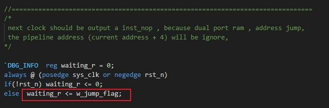
Figure 4 waiting_r

Figure 5 Assign curr_instr to nop
1.3. Digital tube display example and simulation
Figure 6 shows an example disassembly showing the character “F” in a nixie tube. Obviously, before the tag <START>, the pipeline fetches, executes and writes back each instruction sequentially. However, there is a branch conditional instruction at address 8000_003c. If the condition is met, the PC will jump to 8000_0038 instead of 8000_0040. When the pipeline has fetched the instruction at address 8000_0040, special attention should be paid to its execution result.

Figure 6 Jump example
The simulation results are shown in Figure 7. It can be seen that when curr_instr is 0x0000_0001, that is , when curr_instr is assigned as nop, i_PC will change from 0x8000_0040 to 0x8000_0038 with a delay. As mentioned before, the jump flag will change curr_instr from any instruction to ʻINST_NOP (0x0000_0001).

Figure 7 Simulation results
1.4. UART serial output example and simulation
Figure 8 shows another UART example. It outputs “This is a call function program” from the UART. Figure 9 shows the printout information stored in the rodata section. When the pipeline executes instruction 0x8000_0044, the instruction at address 0x8000_0048 has already been fetched. However, according to the 0x8000_0044 instruction, the PC should point to 0x8000_0078 to load the print data. At this point, the PC will abandon the instruction at address 0x8000_0048 and keep the address until 0x8000_0078 rodata is loaded, and the PC will return the address pointing to 0x8000_0048. Figure 10 shows the simulation results for the UART example. It can be seen that curr_instr has been assigned to INST_NOP (0x0000_0001) after giving up the instruction at address 0x8000_0048.

Figure 8 UART example

Figure 9 Output printing information

Figure 10 Simulation results
1.5. Long-cycle memory access instruction processing
Assign instr_fch_PC (PC+4) to next_addr before assigning the actual address to the PC , because after the load/store is performed, the normal PC+4 address will be the next PC to execute, as shown in Figure 11. Figure 12 is the same as Figure 2, but with rib_delay_op highlighted here . This is a decision-making judgment. If the current instruction is a long-cycle load and store, next_addr is assigned to instr_fch_PC , and when a long-cycle load and store is performed, next_addr is assigned to i_PC .

Figure 11 Assign instr_fch_PC to next_addr

Figure 12 Long Cycle Load & Store