1. RESET the result before generating the *.bit file
First, open the Vivado FII_RISCV_V2.01 project (here, the V2.01 version is used as an example), as shown in Figure 1.

Figure 1 FII_RISCV_V2.01 project
To generate the corresponding *.bit file, synthesis and implementation are required first. It is recommended to reset the previous result before performing synthesis. The Reset operation is shown in Figure 2-Figure 4.
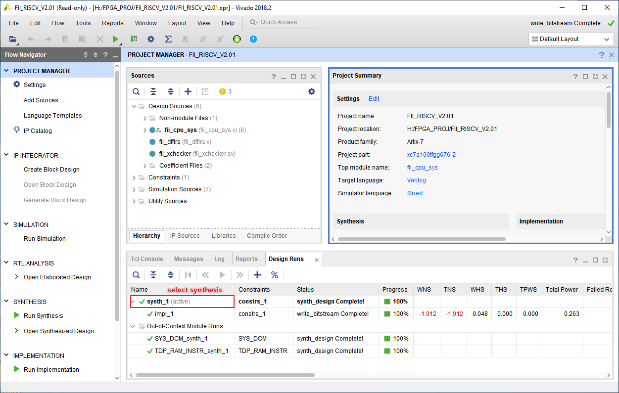
Figure 2 Select the last synthesis

Figure 3 Select reset

Figure 4 Confirm reset in the pop-up window
2. Generate *.bit file
Click Generate Bitstream to generate a *.bit file, as shown in Figure 5.
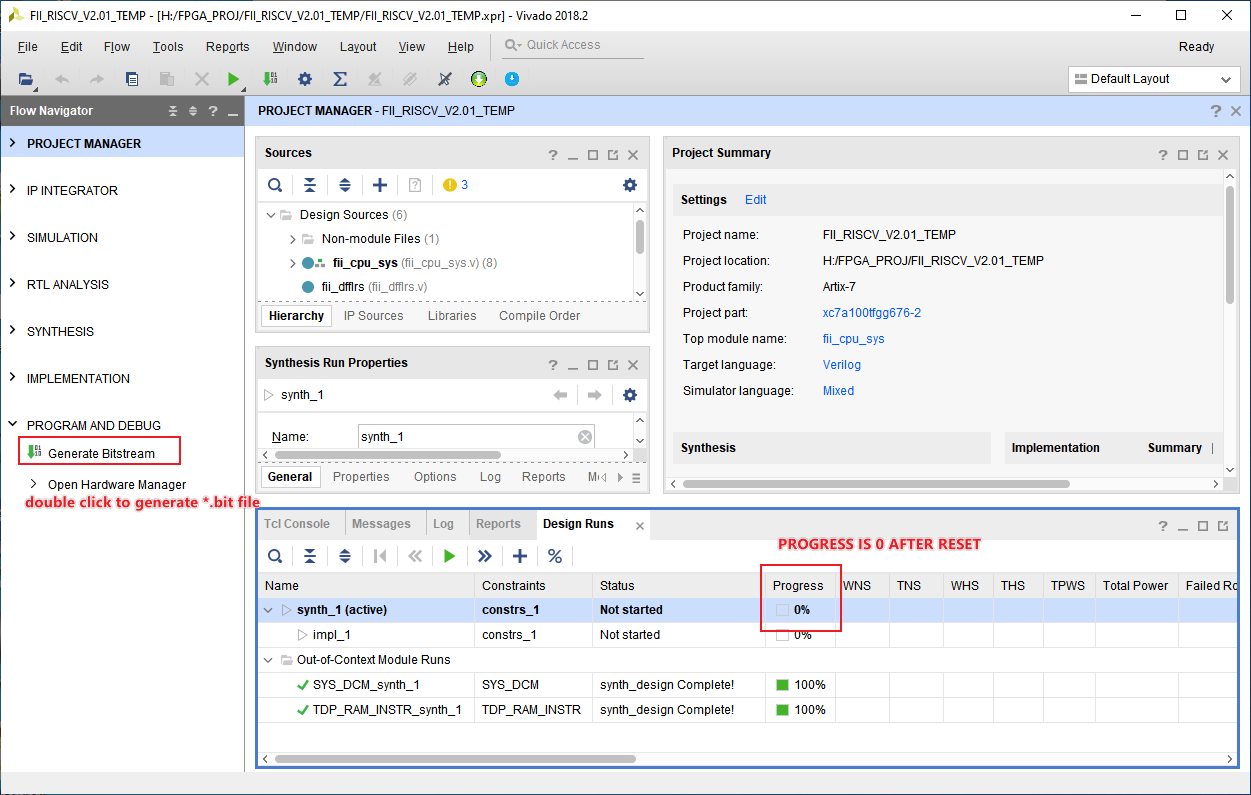
Figure 5 Generate *.bit file
After the *.bit file is successfully generated, the window shown in Figure 6 will appear. Select Open Hardware Manager to program the FPGA.

Figure 6 Successfully generated *.bit file
3. Burn the *.bit file
In the Hardware Manager interface, there are 1 and 2 methods to open target , as shown in Figure 7.

Figure 7 open target
Click Open Target , the window shown in Figure 8 appears, click Auto Connect .

Figure 8 Auto Connect
After Auto Connect, the PRX100-D chip, xc7a100t, will appear in the Hardware Manager window, as shown in Figure 9.

Figure 9 Connection to PRX100-D chip
As shown in Figure 10, click xc7a100t, and then click Program Device .

Figure 10 Program Device
As shown in Figure 11, select the correct *.bit file in the pop-up window . Click in the green box to select the *.bit file in the interface shown in Figure 12. After selecting the *.bit file, click Program .

Figure 11 Select the correct *.bit file

Figure 12 Select the correct *.bit file
4. Generate *.mcs file
Click Tools > Generate Memory Configuration File on the Vivado menu , as shown in Figure 13.

Figure 13 Tools > Generate Memory Configuration File
After the window shown in Figure 14 pops up, configure it according to the following steps:
- Select format as MCS
- Select Memory Part, mt25ql128 (select the corresponding FLASH in the green box)
- Name the *.mcs file to be generated
- According to the configuration of the *.xdc file, select SPIx1, SPIx2 or SPIx4, here the interface is selected as SPIx4 , if there is no SPI configured in the *.xdc file, SPIx1 is selected by default
- Select Load bitstream files
- Select the generated *.bit file in the green box
- select Overwrite
- Click OK

Figure 14 Generate *.mcs file
After the *.mcs file is successfully generated, the window shown in Figure 15 will pop up, click OK in the green box.

Figure 15 Successfully generated *.mcs file
5. Burn the *.mcs file
The *.mcs file is called Intel MCS-86 Hexadecimal Object, and the format has a 9-character (4-field) prefix that defines the start of the record, the number of bytes, the load address, and the record type, and a 2-character Checksum suffix.
The following figure shows the indirect programming of FLASH through JTAG through FPGA. When the programming is completed, the FPGA loads the program from the FLASH after power-on.

Before burning the *.mcs file, you need to add FLASH, as shown in Figure 16. Click on xc7a100t in Hardware Manager and click on Add Configuration Memory Device .

Figure 16 Add configuration memory device
In the pop-up window shown in Figure 17, enter mt25ql128 .

Figure 17 Selecting the memory device
After selecting the memory device, the pop-up window shown in Figure 18 will appear, click OK. Or in the Hardware Manager shown in Figure 19, click mt25ql128 , click Program Configuration Memory Device

Figure 18 Pop-up window

Figure 19 Click to configure memory
In the pop-up window shown in Figure 20, you can burn the *.mcs file through the following steps:
- Select the *.mcs file generated before, click the green box to select and configure
- Program is required , other options are optional
- Click OK

Figure 20 Select the *.mcs file
So far, the process of burning the *.mcs file to FLASH has been completed. The PRX100-D development board will be in an idle state (that is, the FPGA is not working), you can activate the FPGA by pressing the reset button on the FPGA board (or power off, and then power on to start the FPGA program in the FLASH).
6. Software Compilation Environment and Lower Board Experiment
There are previous articles describing the relevant steps, see the following articles:
- RISC-V Assembly Language Programming (3) Compilation Environment and Board Experiment
- RISC-V asm_compile tool uses
7. Hardware connection
7.1 Two USB-b male cables + FII-PRX100-D development board
If there are two USB-b male connectors, as shown in Figure 21, you can burn *.bit files or *.mcs files during the normal burning process.

Figure 21
7.2 A USB-b male cable + FII-PRX100-D development board
If there is only one USB-b male cable, you should connect the cable to CPU_JTAG first, as shown in Figure 22, and burn the *.mcs file.

Figure 22
Then connect the line to the USB TO UART, as shown in Figure 23, to complete the software down-board experiment.

Figure 23